Introduction
I/O interfaces are the mediums through which data is sent from internal logic to external sources and received from external sources. The interface signals can be unidirectional or bidirectional, only one ended or differential, and adhere to one of several I/O standards. The I/O interfaces' primary function is to send and receive signals; however, the fraction assigned as an I/O interface may contain additional resources such as voltage translators, registers, impedances, and buffers.
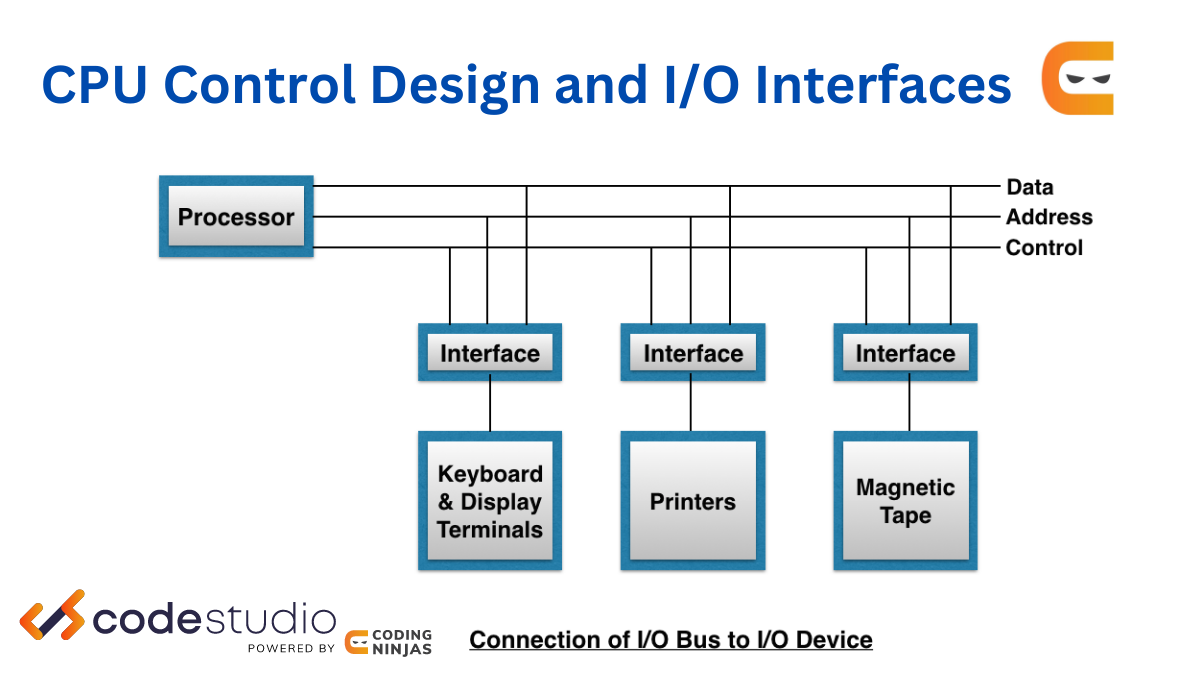
Or in other ways, we can say that surfaces are required whenever a CPU communicates with I/O devices. The interface is used to perceive the address generated by the CPU. Thus, the surface is used to communicate with I/O devices, i.e. to share data between CPU and I/O devices, an interface called I/O Interface is used.
Here in this blog, we will look into the most important CPU control design and io interfaces questions.
CPU Control Design and IO Interfaces Questions

Let us now start discussing all the important questions in this section.
1. Consider the following sequence of micro-operations.
MBR ← PC
MAR ← X
PC ← Y
Memory ← MBR
Which one of the following is a possible operation performed by this sequence?
- Instruction fetch
- Operand fetch
- Conditional branch
-
Initiation of interrupt service
Ans: The answer to this question is option D. MBR stands for Memory Buffer Register ( that stores the data being transferred to and from the immediate access store) Memory Address Register (MAR) ( that holds the memory location of data that needs to be accessed.) PC stands for Program Counter ( It contains the address of the instruction being executed at the current time ).
The first instruction inserts the value PC into MBR. The second instruction inserts address X into MAR. The third instruction enters the address Y into the PC. The fourth instruction stores the value of MBR (the old PC value) in Memory.
2. The amount of ROM needed to implement a 4-bit multiplier is
- 64 bits
- 128 bits
- 1 Kbits
-
2 Kbits
Ans: The answer to this question is D because there are 24 * 24 combinations, or 28 combinations, for a 4-bit multiplier. In addition, the output of a four-bit multiplier is eight bits. Thus, the required ROM is 28 * 8 = 211 = 2048 bits = 2Kbits.
3. The use of multiple register windows with overlap causes a reduction in the number of memory accesses for
I. Function locals and parameters
II. Register saves and restores
III. Instruction fetches
- I only
- II only
- III only
-
I, II, and III
Ans: The correct option is A because using multiple register windows eliminates the need to repeatedly access variable values from memory. We instead keep them in the registers.
4. Consider the main memory system that consists of 8 memory modules attached to the system bus, which is one word wide. When a write request is made, the bus is occupied for 100 nanoseconds (ns) by the data, address, and control signals. During the same 100 ns, and for 500 ns thereafter, the addressed memory module executes one cycle accepting and storing the data. The (internal) operation of different memory modules may overlap in time, but only one request can be on the bus at any time. The maximum number of stores (of one word each) that can be initiated in 1 millisecond is ____________
- 1000
- 10000
- 100000
-
100
Ans: the correct answer is B because one request takes 100ns. So the total number of requests that can be started is 1000000 ns/100 ns = 10000.
5. Which of the following is true for a CPU with a single interrupt request line and a single interrupt grant line?
- Neither vectored interrupt nor multiple interrupting devices are possible.
- Vectored interrupts are not possible but multiple interrupting devices are possible.
- Vectored interrupts and multiple interrupting devices are both possible.
-
Vectored interrupt is possible but multiple interrupting devices are not possible.
Ans: The correct answer is option C because it depends on the kind of CPU we use.
6. Consider the following data path of a simple non-pipelined CPU. The registers A, B, A1, A2, MDR, the bus, and the ALU are 8-bit wide. SP and MAR are 16-bit registers. The MUX is of size 8 × (2:1) and the DEMUX is of size 8 × (1:2). Each memory operation takes 2 CPU clock cycles and uses MAR (Memory Address Register) and MDR (Memory Data Register). SP can be decremented locally.
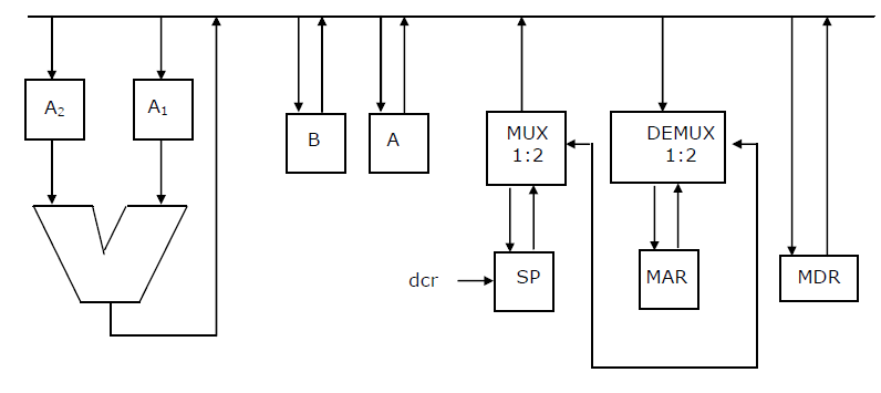
The CPU instruction “push r”, where = A or B, has the specification
M [SP]
How many CPU clock cycles are needed to execute the “push r” instruction?
- 1
- 3
- 4
-
5
Ans: The correct answer is option B because Push 'r' is made up of the following operations: M[SP]! R SP! SP-1 'r' is currently stored in memory at the address stack pointer, which takes two clock cycles. SP is then decremented to point to the next stack top. As a result, total cycles=3.
7. What is the minimum size of ROM required to store the complete truth table of an 8-bit x 8-bit multiplier?
- 32 K x 16 bits
- 64 K x 16 bits
- 16 K x 32 bits
-
64 K x 32 bits
Ans: The correct answer is option B because Input to ROM - two 8-bit lines In ROM, possible combinations are (2^8)x(2^8). Truth table size = (2^8)*(2^8)=2^16=64 KB The maximum output size is 16 bits.
8. A CPU has only three instructions I1, I2, and I3, which use the following signals in time steps T1-T5: I1: T1: Ain, Bout, Cin T2: PCout, Bin T3: Zout, Ain T4: Bin, Cout T5: End I2 : T1: Cin, Bout, Din T2: Aout, Bin T3: Zout, Ain T4: Bin, Cout T5: End I3: T1: Din, Aout T2: Ain, Bout T3: Zout, Ain T4: Dout, Ain T5: End Which of the following logic functions will generate the hardwired control for the signal Ain?
- T1.I1 + T2.I3 + T4.I3 + T3
- (T1 + T2 + T3).I3 + T1.I1
- (T1 + T2 ).I1 + (T2 + T4).I3 + T3
-
(T1 + T2 ).I2 + (T1 + T3).I1 + T3
Ans: The correct answer is option A.
9. A hardwired CPU uses 10 control signals S1 to S10, in various time steps T1 to T5, to implement 4 instructions I1 to I4 as shown below: table which of the following pairs of expressions represent the circuit for generating control signals S5 and S10 respectively? ((Ij+Ik)Tn indicates that the control signal should be generated in time step Tn if the instruction being executed is Ij or lk)
- S5=T1+I2⋅T3 and S10=(I1+I3)⋅T4+(I2+I4)⋅T5
- S5=T1+(I2+I4)⋅T3 and S10=(I1+I3)⋅T4+(I2+I4)⋅T5
- S5=T1+(I2+I4)⋅T3 and S10=(I2+I3+I4)⋅T2+(I1+I3)⋅T4+(I2+I4)⋅T5
-
S5=T1+(I2+I4)⋅T3 and S10=(I2+I3)⋅T2+I4⋅T3+(I1+I3)⋅T4+(I2+I4)⋅T5
Ans: The correct answer is option D.
10. n instruction set of a processor has 125 signals which can be divided into 5 groups of mutually exclusive signals as follows:
Group 1: 20 signals, Group 2: 70 signals, Group 3: 2 signals, Group 4: 10 signals, Group 5: 23 signals.
How many bits of the control words can be saved by using vertical microprogramming over horizontal microprogramming?
- 0
- 103
- 22
-
55
Ans: The correct option is B. Each control signal in horizontal microprogramming is depicted by one bit in the microinstruction. As a result, the total number of bits required for control words in horizontal microprogramming is = 20 + 70 + 2 + 10 + 23 = 125 bits.
Vertical microprogramming encodes 'n' control signals into log2 n bits.
log2 20 = 5 bits in group 1
log2 70 = 7 bits in group 2
log2 2 = 1 bit in group 3
log2 10 = 4 bits in group 4
log2 23 = 5 bits in group 5
Vertical microprogramming requires a total of 5 + 7 + 1 + 4 + 5 = 22 bits.
So the total number of bits saved is 125 - 22 = 103 bits.
11. Which one of the following facilitates the transfer of bulk data from hard disk to main memory with the highest throughput?
- DMA-based I/O transfer
- Interrupt driven I/O transfer
- Polling-based I/O transfer
-
Programmed I/O transfer
Ans: The correct answer is option A. DMA transfers large amounts of data from secondary storage to primary memory without the use of a CPU.
12. A computer handles several interrupt sources which of the following are relevant for this question.
Interrupt from CPU temperature sensor (raises interrupt if CPU
temperature is too high)
Interrupt from Mouse (raises interrupt if the mouse is moved or a button is
pressed)
Interrupt from Keyboard (raises interrupt when a key is pressed or released)
Interrupt from Hard Disk (raises interrupt when a disk read is completed)
Which one of these will be handled at the highest priority?
- Interrupt from hard disk
- Interrupt from mouse
- Interrupt from keyboard
-
Interrupt from the CPU temperature sensor
Ans: The correct answer is D.


 9+ registered