Do you think IIT Guwahati certified course can help you in your career?
Introduction
A flip-flop is a one-bit memory cell that can store digital content. A collection of flip-flops must be used to improve the storage capacity in terms of bits. A Register is a collection of such flip-flops. The n-bit register has n flip-flops and can hold an n-bit word.
A shift register is a collection of flip-flops that stores numerous pieces of information. With the use of shift registers, the data held in these registers can be transferred. Clock pulses can be used to make the bits contained in such registers move inside them and in and out of them.
"Shift left registers" shift the bits to the left.
"Shift right registers" shift the bits to the right.
What is a Register?
A register is a small, fast storage location within the CPU (Central Processing Unit) of a computer. It is used to store and quickly retrieve data that is actively being processed or manipulated by the CPU. Registers are essential for performing arithmetic and logical operations, holding intermediate results, and storing memory addresses during program execution.
The size and number of registers can vary between different CPU architectures, impacting the overall performance and efficiency of a computer's processing capabilities.
What are Shift registers in digital electronics?
Shift registers are digital circuits used in digital electronics for the storage and manipulation of binary data. They consist of a series of flip-flops connected in a chain, with the output of one flip-flop connected to the input of the next flip-flop.
Types of Shift Registers
There are six types of shift registers which are:
Serial In Serial Out shift register
Serial In parallel Out shift register
Parallel In Serial Out shift register
Parallel In parallel Out shift register
Bidirectional Shift Register
Universal Shift Register
Let us learn thoroughly about each one of them.
1. Serial In Serial Out Shift Register (SISO)
A shift register that receives serial input (one bit at a time across a single data line) and outputs serial data is a serial-in serial-out shift register. The data exits the shift register one bit at a time in a serial pattern since there is only one output, thus the term Serial-In Serial-Out Shift Register.
The SISO shift register is the simplest of the four types since it only has three connections: a serial input (SI) that decides what goes into the left-hand flip-flop, a serial output (SO) that comes from the right-hand flip-flop output, and a sequencing clock signal (Clk). The logic circuit schematic below shows a generalized serial-in serial-out shift register (SISO).
Block Diagram
Working
The outputs Y3, Y2, Y1, Y0 equal 0000 when the clock signal application is deactivated. The LSB bit is given to the data input Din, DA. We'll use the clock this time, and DA's value will be 1. The first flip flop, FF-A, is set at the first falling edge of the clock, and the word is put in the register. The saved word is now 1000.
The data input DB receives the next bit of the binary integer, i.e., 1. FF-B's second flip flop is set when the clock's next negative edge strikes, and the word is saved. The value of the stored word has been changed to 1100.
The clock is applied when the next bit of the binary number, 1, is sent to the data input DC. The third flip flop, FF-C, is set when the clock's negative edge strikes again, and the word is saved. 1110 is substituted for the previously-stored word.
The clock is also applied when the last bit of the binary number, 1, is sent to the input DD. When the negative edge of the clock comes, the last flip flop, FF-D, is set, and the word is saved. 1111 replaces the previously-stored word.
2. Serial In Parallel Out shift Register (SIPO)
Serial-In Parallel-Out shift registers accept serial input and output (one bit at a time over a single data line).
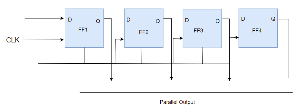
The logic circuit below shows a serial-in-parallel-out shift register. The circuit consists of four D flip-flops that are connected. In addition to the clock signal, the clear (CLR) signal is used to RESET the flip-flops. The output of the first flip-flop is connected to the input of the second flip-flop, and so on. Each flip flop is synced since they all get the same clock signal.
Bit by bit, data is loaded. While the data is loaded, the outputs are disabled.
When all flip-flops have their requisite data, and the data loading is complete, the outputs are activated. All of the loaded data is made available simultaneously over all of the output lines.
Block diagram
Working
Assume that all of the flip-flops (FFA to FFD) have been RESET (CLEAR input) and that all of the outputs (QA to QD) are at logic level "0," i.e., no parallel data output.
If a logic "1" is connected to FFA's DATA input pin, the output of FFA, and hence the consequent QA, will be set HIGH to logic "1" on the first clock pulse, with all other outputs staying LOW at logic "0." Assume that the FFA's DATA input pin has now been reset to logic "0," giving us one data pulse or 0-1-0.
Because its input D has the logic "1" level on it from QA, the second clock pulse will convert the output of FFA to logic "0" and the output of FFB and QB HIGH to logic "1." As it is currently at QA, logic "1" has been relocated or "shifted" one position along with the register to the right.
The logic "1" value goes to the output of FFC (QC) when the third clock pulse comes, and so on until the fifth clock pulse arrives, which resets all the outputs QA to QD to logic level "0" since the input to FFA has stayed constant at logic level "0."
Each clock pulse causes the data contents of each stage to shift one position to the right until the entire data value of 0-0-0-1 is stored in the register. This data value can now be directly read from the QA to QD outputs.
3. Parallel In Serial Out Shift Register (PISO)
Shift registers with parallel input and serial output allow parallel input (data is sent to each flip flop separately and concurrently) and produce a serial output.
The circuit consists of four D flip-flops that are connected. The clock input connects to all the flip-flops directly, whereas the input data is connected to each flip-flop individually with the multiplexer. The previous flip flop's output and parallel data input are connected to the MUX's input, while the MUX's output is connected to the next flip flop. The logic circuit below shows a parallel-in-serial-out shift register.
Block diagram
Working
There are two modes in which the "PISO" circuit operates, shift mode and load mode.
Load Mode
The 2, 4, and 6 AND gates become active when the shift/load bar line is low (0), and they transmit B1, B2, B3 bits to the associated flip-flops. The binary inputs B0, B1, B2, and B3 will be fed into the respective flip-flops on the low going edge of the clock. As a result, parallel loading occurs.
Shift Mode
When the load and shift lines are set to 0, the second, fourth, and sixth gates remain inactive. As a result, we are unable to load data in parallel. The 1st, 3rd, and 5th gates will now be turned on, and the data will be shifted to the right bit. The "Parallel IN Serial OUT" procedure is performed in this manner.
4. Parallel In Parallel Out Shift Register (PIPO)
The parallel-In parallel-Out shift register is a shift register that permits parallel input (data is delivered independently to each flip flop and simultaneously) and provides a parallel output.
The PIPO shift register has just three connections:
A parallel input (PI) decides what goes into the flip-flop.
A parallel output (PO).
A sequencing clock signal (Clk).
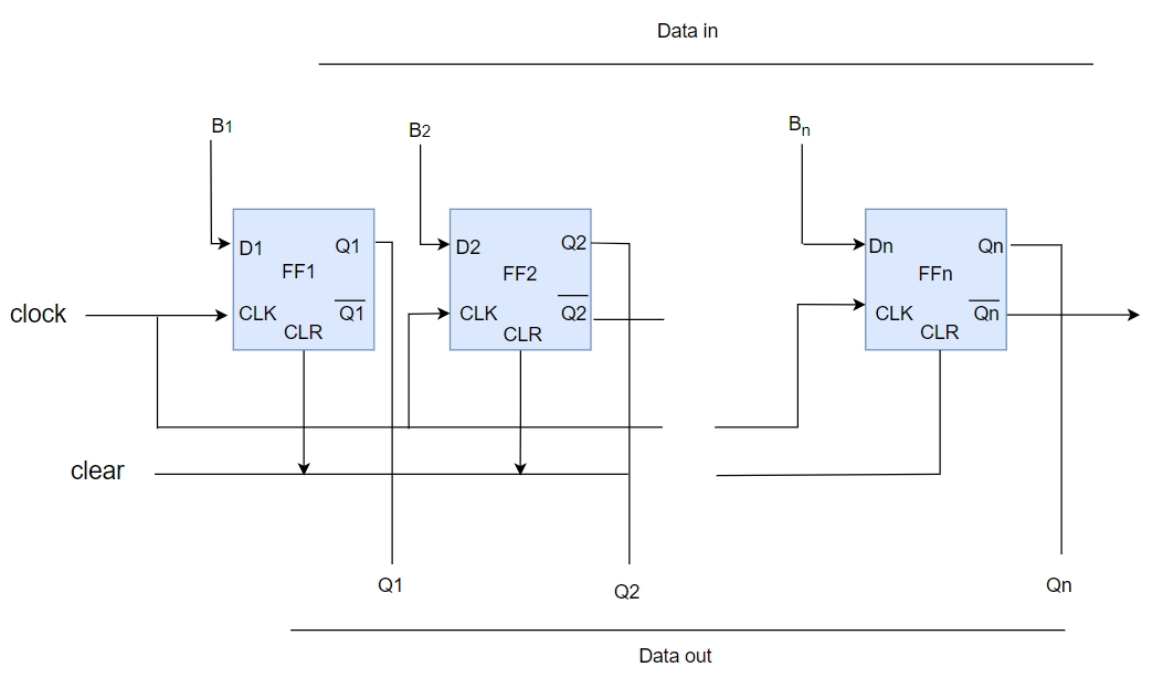
The circuit consists of four D flip-flops that are connected. The clear (CLR) and clock signals are coupled to all four flip flops. There are no links between the individual flip-flops in this register since serial data shifting is not required. As input, data is provided to each flip flop separately, and output is also collected separately from each flip flop. The logic circuit below shows a parallel-in-parallel-out shift register.
Block diagram
Working
At the first clock pulse point, each flip-flop stores an individual bit of the data as its input (FF1 stores B1 appearing at D1; FF2 stores B2 appearing at D2... FFn stores Bn appearing at Dn). Furthermore, the bit stored in each flip-flop simultaneously appears at its corresponding output pins (Q1 = D1; Q2 = D2 & Qn = Bn). This means that with PIPO registers, both data store and data recovery happen on a single (and simultaneous) clock pulse.
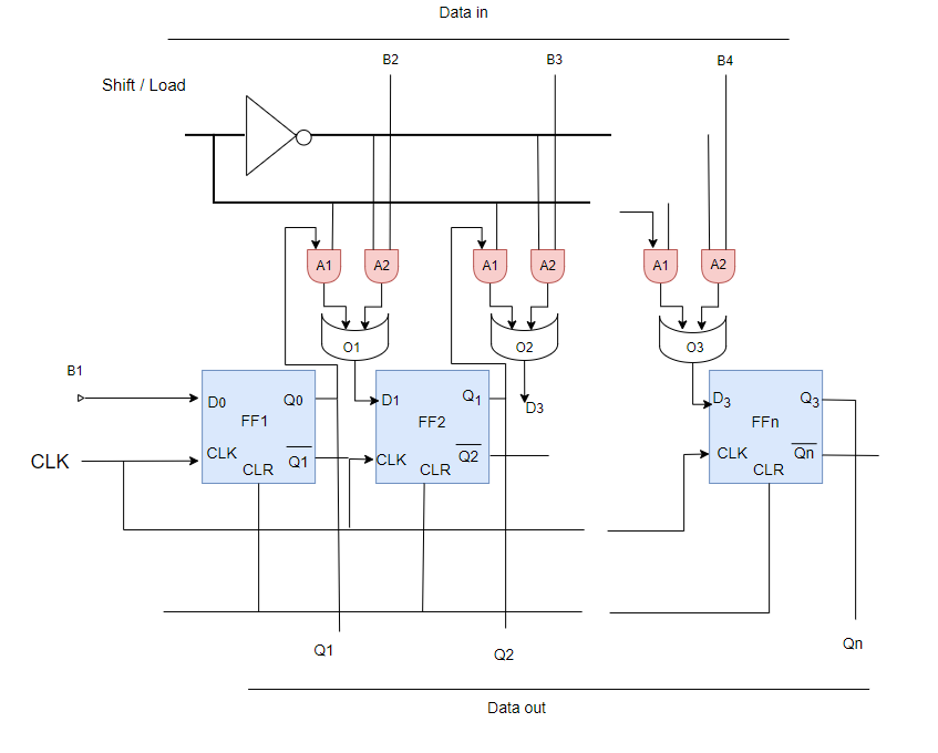
It is important to note that the PIPO register in the above figure cannot move data bits. In order to turn the PIPO register shown above into a PIPO shift register, the circuit must be modified by adding the combinational circuit and control lines SH/LD` (SHIFT/~LOAD) as shown below.
PIPO shift register with combinational circuit and control line
If the SH/LD` line is low, all combinational circuits' A2 AND gates become active, while A1 gates become dormant. As a result, the bits of the input data word (Data in) that appear as inputs to the gates A2 are passed on as OR gate outputs, which are then loaded/stored in corresponding flip-flops when the first leading edge of the clock appears (except the bit B1 which gets directly stored into FF1 at the first clock tick). This means that at the same clock pulse, all the bits of the input data word are stored in the register components. These bits emerge on the output pins of the corresponding flip-flops simultaneously, resulting in a parallel-output data word at the same clock tick.
Furthermore, when the SH/LD` line is high, all combinational circuits' A1 gates are enabled, while A2 gates are deactivated. The output bit of each flip-flop appears at the output of the OR gate, driving the very-next flip-flop. As a result of this (except the last flip-flop FFn) FF1's output bit (Q1) becomes the output of OR gate 1 (O1) linked to D2; Q2 becomes the output of O2 = D3; and so on. If the rising edge of the clock pulse emerges at this point, Q1 will appear at Q2, Q2 will appear at Q3,..., and Qn-1 will appear at Qn. This is nothing more than a one-bit right-shift of the data stored in the register. Truth Table given below underlines the importance of this effort.
5. Bidirectional Shift Register
A Bidirectional Shift Register (BDSR) is a type of digital circuit used for data storage and manipulation. It consists of a series of flip-flops or other memory elements connected in series, with the output of one flip-flop serving as the input to the next. The data stored in a BDSR can be shifted in either direction, left or right, allowing for efficient manipulation of the stored data.
Block diagram
Working
A Bidirectional Shift Register (BDSR) works by shifting the stored data in either direction, left or right, based on the control signals applied to the BDSR. The BDSR consists of a series of flip-flops or other memory elements, with the output of one flip-flop serving as the input to the next.
In a left shift operation, the data stored in the BDSR is shifted to the left by one bit, with the least significant bit being lost and the most significant bit is shifted into the next flip-flop. The direction of the shift is determined by a control signal, such as a shift control line, which is used to activate the left shift operation.
In a right shift operation, the data stored in the BDSR is shifted to the right by one bit, with the most significant bit being lost and the least significant bit is shifted into the next flip-flop. The direction of the shift is determined by a control signal, such as a shift control line, which is used to activate the right shift operation.
6. Universal Shift Register
A Universal Shift Register (USR) is a type of digital circuit that can perform both left and right shifts, as well as parallel loading of data. This makes the USR a versatile component that can be used in a variety of applications, such as data storage, serial-to-parallel conversion, and parallel-to-serial conversion.
Block diagram
Working
A Universal Shift Register (USR) works by shifting the stored data in either direction, left or right, based on the control signals applied to the USR. The USR also allows for the parallel loading of data.
The USR consists of a series of flip-flops or other memory elements, with the output of one flip-flop serving as the input to the next. The USR also has additional control inputs, such as load, shift, and direction control signals, that determine the operation performed by the USR.
In a left shift operation, the data stored in the USR is shifted to the left by one bit, with the least significant bit being lost and the most significant bit is shifted into the next flip-flop. The direction of the shift is determined by a control signal, such as a shift control line, which is used to activate the left shift operation.
In a right shift operation, the data stored in the USR is shifted to the right by one bit, with the most significant bit being lost and the least significant bit is shifted into the next flip-flop. The direction of the shift is determined by a control signal, such as a shift control line, which is used to activate the right shift operation.
In a parallel load operation, new data is loaded into the USR simultaneously, with each flip-flop receiving a new input. This operation is performed by activating the load control signal, which applies the new data to the inputs of the flip-flops in the USR.
Performing data alignment and reordering in digital systems.
Converting incoming serial data to a parallel format for processing.
Converting parallel data to a serial format for transmission.
Introducing a fixed delay to a digital signal for synchronization purposes.
Implementing simple digital filters.
Frequently Asked Questions
What are shift registers used for?
Shift registers are used for:
Data Storage: It can be used to store data.
Data Transfer: It can be used to transfer data between different parts
Data Shift and Rotation: It can be used to perform bitwise operations such as shift and rotate on data.
What are the basic types of shift register?
Basic shift registers include Serial-In, Serial-Out (SISO), Serial-In, Parallel-Out (SIPO), Parallel-In, Serial-Out (PISO), and Parallel-In, Parallel-Out (PIPO).
What are parallel and shift registers explain?
Parallel registers process data simultaneously, while shift registers move data sequentially, shifting it bit by bit through the register.
What is universal shift register?
A universal shift register can operate in all modes (SISO, SIPO, PISO, PIPO), providing versatile data shifting capabilities for various applications in digital circuits.
Conclusion
In this article, we have discussed about Shift Registers in Digital Electronics. The exploration of shift registers in digital electronics unveils their pivotal role in data storage, manipulation, and transfer. From the fundamental SISO to the versatile universal shift register, these components form the backbone of various applications, contributing to the efficiency and functionality of digital circuits
We hope that this blog has helped you enhance your knowledge regarding different register types with their specific working and circuitry, along with their waveforms. If you would like to learn more, check out our articles on computer architecture and counters in digital logic and more by looking at our other connected articles on Code Studio. Do upvote our blog to help other ninjas grow. Happy Coding!
Live masterclass
Resume & linkedin tips to crack Amazon GenAI Interviews
by Anubhav Sinha
30 Jul, 2026
12:30 PM
Master PowerBI using Flipkart Dataset & Ace 20LPA+ Data Roles
by Prerita Agarwal
27 Jul, 2026
12:30 PM
Multi-Agent AI Support Bot using OpenAI & Gemini
by Saurav Prateek
28 Jul, 2026
12:30 PM
Zomato Data Analysis Case Study: Ace 25L+ Roles in FoodTech(no use)
by Abhishek Soni
29 Jul, 2026
11:30 AM
Zomato Sales Analytics: SQL + PowerBI for 25LPA Jobs
by Abhishek Soni
29 Jul, 2026
11:30 AM
Resume & linkedin tips to crack Amazon GenAI Interviews
by Anubhav Sinha
30 Jul, 2026
12:30 PM
Master PowerBI using Flipkart Dataset & Ace 20LPA+ Data Roles


 9+ registered