Table of contents
1.
Introduction
2.
SR Flip Flop 
2.1.
Truth table and Operation
3.
Clocked SR Flip Flop
4.
Debounce circuit
5.
FAQs
6.
Key takeaways
Last Updated: Mar 27, 2024

SR flip flop

Author Aryan Raj
0 upvote
Career growth poll
Do you think IIT Guwahati certified course can help you in your career?

Introduction

Flip flops are an application of logic gates. With Boolean logic, you can create a memory with them. Flip-flops can also be considered the most basic idea of RAM(Random Access Memory). When a specific input value is allotted to them, they will be remembered and executed if the logic gates are designed correctly. Latches and Flip-flops are fundamental building blocks of digital electronics systems used in computers, communications, and various other types of systems.  A higher application of flip-flops helps in designing better electronic circuits.

Flip flops are of the following types:


In this blog. we will learn about SR Flip Flop with its application.

SR Flip Flop 

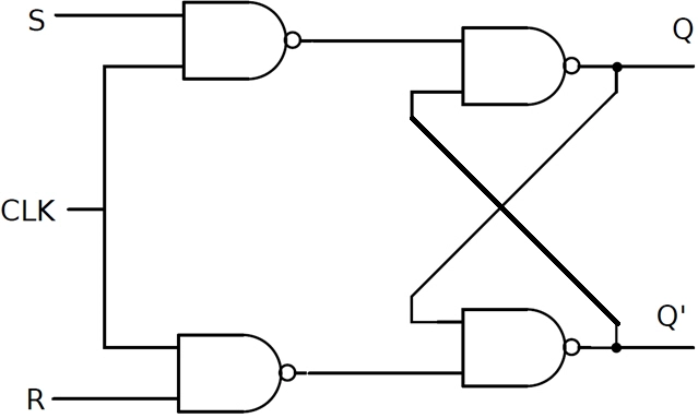
SR (Set-Reset) flip flop is the simplest possible memory element. It can be constructed from two NOR gates or two NAND gates. Let us understand the operation of the SR flip flop using NOR Gates, as shown in the figure below. 

The inputs S and R are the Set and Reset inputs, respectively. The outputs Q and Q' are both complements of each other and are referred to as the normal and complement outputs, respectively. 

Flop can be constructed by any of the two types of Latches, but the best practice is to use NAND gate Latch. 


The condition of the output Q determines the state of the Set-Reset flip flop. 

  • When the outputs are Q'=0 and Q=1, it is in the set state (or 1-state). 
  • When the outputs are Q'=1 and Q=0, it is in the reset/clear state (or 0-state).


The SET inputs are labeled as S, and RESET inputs are labeled as R, respectively.

The SR flip flop can be constructed using NOR gates or NAND gates. 

Truth table and Operation


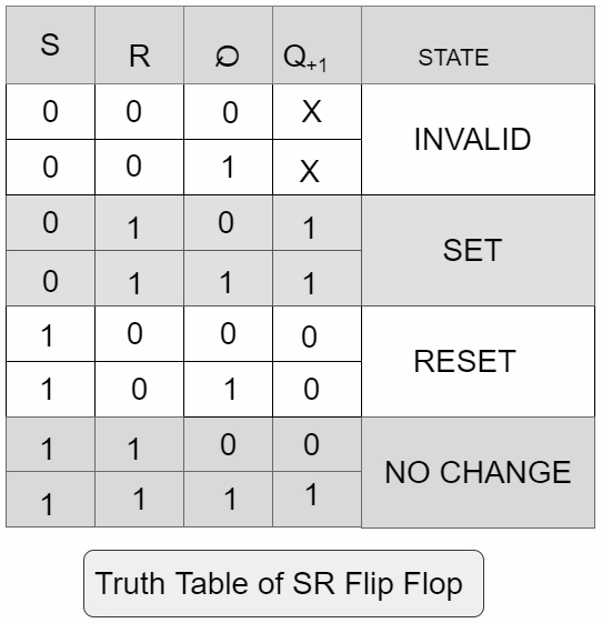
Case 1: (S=1 and R=0): The output of the bottom NOR gate is equal to 0(zero), Q'=0. Since both inputs to the top NOR gate are equal to 0(Zero), thus, Q=1. So, the input combination R=0 and S=1 leads to the flip-flop being set to Q=1.

Therefore, whether the present state output is either 1 or 0, the subsequent state output is logic 1(one), which will SET the flip flop.

Case 2: (S=0 and R=1): Similar to the above arguments, the outputs become Q'=1 and Q=0. We say that the flip-flop is reset.

So, therefore, whether the present state is either 1 or 0, it will produce an output 0, which will RESET the flip flop.

Case 3: (S=0 and R=0): Assume the flip flop was previously in set (R=0 and S=1) condition. Now, changing the value of S to 0 results in Q' still at 0 and Q=1. Similarly, when the flip flop was previously in a reset state (R=1 and S=0), the outputs do not change. Therefore, with inputs R=0 and S=0, the flip-flop holds its state.

For these inputs, the output we get by the NAND gate is Q+1 = 1, so there is no change in the state.

Case 4: (S=1 and R=1): This condition will violate the fact that both the outputs are complements of each other. However, each of them will try to go to 0 (zero), which is not a stable configuration. It is impractical to predict which output will go to value 1(one) and which will stay at value 0. In a typical normal operation, this condition must be avoided by ensuring that 1's are not applied to both the inputs simultaneously, thus making it one of the major disadvantages of SR flip flop.

Clocked SR Flip Flop

Clocked SR Flip Flop is also called a Gated SR flip-flop. The problem with SR flip-flops using NAND and NOR gate is the invalid state. This problem can be resolved by using a bistable SR flip flop that will change the outputs when certain invalid states happen, regardless of the condition of the Set or Reset inputs. So for this, a clocked SR flip-flop is designed by adding two AND gates to a basic NOR Gate flip-flop. The circuit diagram and truth table are shown below. 
 

Circuit Diagram of clocked SR flip flop


Qn Qn+1
0 0 0 0 (Hold) 
0 1 0 0
0 0 1 1
0 1 1 Indeterminate
1 0 0 1 (Hold) 
1 1 0 0
1 0 1 1
1 1 1 Indeterminate


As shown below, we can use Clock Pulse as a gate input, making it Clocked Flip flop. 

  • Rising edge Triggered (Positive Edge) 
  • Falling Edge Triggered (Negative Edge)

A CP(clock pulse) is given to the inputs of the AND Gate. When the clock pulse value is ’0′(zero), the outputs of both the AND Gates remain ’0′(zero). As soon a pulse is given the value of CP(clock pulse) turns ’1′(one). 
This makes the values at R and S pass through the NOR Gate flip-flop. But when the values of both R and S values turn ’1′(one), the HIGH value of clock pulse causes both of them to turn to ’0′(zero) for a short moment. As soon as the pulse is removed, the flip-flop state becomes intermediate.

So either of the two states may occur, and it depends on whether the set or reset input of the flip flop remains a ’1′ (one) longer than the transition to ’0′ (zero) at the end of the pulse. Thus, invalid states can be eliminated.

Debounce circuit

An elementary example of using this flip-flop is the debounce circuit. Suppose a piece of electronics is to change state under the action of a mechanical switch. When this switch is moved from position S to R (S=0, R=1), the contacts make and break several times at R before settling to good contact. It is desirable that the electronics should respond to the first contact and then remain stable, rather than switching back and forth as the circuit makes and breaks. This is achieved by SR flip flop, which is reset to Q=0 by the first signal R=1 and remains fixed until the switch is moved back to position S when the signal S=1 sets the flip flop to Q=1. 

Must Read Shift Registers in Digital Electronics

FAQs

  1. Why are flip-flops used?
    The Sequential circuit elements (flip-flops and latches) are commonly used to store information. To be more precise, a flipflop is used to store a single binary bit and has two defined states; one of its two states represents “0”, the other represents “1”.
     
  2. What are the various types of flip-flops?
    There are four different types of flip flops, and these are:
    JK flip-flop.
    Set-Reset (SR) flip-flop or Latch.
    D (Data or Delay) flip-flop.
    T (Toggle) flip-flop.
     
  3. How does a flip-flop store a bit?
    A Flip-flop is used to store only one bit of information, By connecting several Flip-flops together, we may store more data that can represent the value of a counter, the state of a sequencer, an ASCII character in a computer's memory, or any other piece of information.
     
  4. What is the problem with the SR flip flop?
    The problem with Set-Reset flip flops using NAND and NOR gate is the invalid state(Clocked SR Flip Flop). This problem can be resolved using a bistable Set-Reset(SR) flip-flop that can change outputs when something invalid states occur, regardless of the condition of either the Reset or the Set inputs.

Key takeaways

In this blog, we have discussed  SR flip flop and its application, we have also covered debounce circuit and clocked SR flip flop along with its truth table.

If you are pursuing a new career and are interested in exploring fields like web development, and want to learn DSA, you can look for our Guided path for DSA, which is free!  

Happy Learning, Ninja!

Live masterclass