Introduction
Instructions are the order which is given by the user to the computer to perform some specific function desired. Mostly the codes of the instruction are written in binary language, i.e: 0’s and 1’s. ADD, JUMP, LOAD, etc are some of the instructions used in processors.

In this blog, we will discuss the Instructions Types. They are classified into three types:
- Memory reference instruction
- Register reference instruction
- Input Output instruction

Types of Basic Computer Instructions
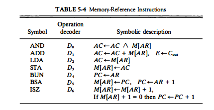
Memory Reference Instruction
These instructions are mainly used to perform operations on operands that are located in memory.
From bit 0 to bit 11, represent the address field that specifies the operand's address. From bit 12 to bit 14 represent the opcode field which consists of 7 operations as 3 bits are used to specify it. The 15th bit specifies the indirect bit. If I=0, this means direct address and I = 1 means indirect address. (figure a).
Below are the memory reference instructions.
| Instruction | I=0 | I=1 | Description |
| AND | 0XXX | 8XXX | Performs AND operation between memory and accumulator. |
| ADD | 1XXX | 9XXX | Performs add operation between memory and accumulator. |
| LDA | 2XXX | AXXX | Load accumulator in memory |
| STA | 3XXX | BXXX | Store accumulator in memory |
| BUN | 4XXX | CXXX | Branch unconditionally |
| BSA | 5XXX | DXXX | Branch and save return address |
| INC | 6XXX | EXXX | Increment |
Address is written in hexadecimal notation.
AND instruction is executed when decoder output is D0 and timing signal is T4.
To perform AND operation, we transfer the memory content to the data register, and in the next clock, the operation is performed on the data register and accumulator.
D0T4: DR←M[AR]
D0T5: AC Ʌ DR, SC←0
ADD instruction is executed when decoder output is D0 and timing signal is T5.
To perform ADD operation, we transfer the memory content to the data register, and in the next clock, the operation is performed on the data register and accumulator.
D1T4: DR←M[AR]
D1T5: AC ← AC+DR, E←Cout, SC←0
LDA instruction is executed when decoder output is D2 and timing signal is T4.
To perform the LDA operation, we transfer the content of memory to the data register, and in the next clock, the contents of the data register are transferred to the accumulator.
D2T4: DR←M[AR]
D2T5: AC ← DR, SC←0
STA instruction is executed when decoder output is D3 and timing signal is T4.
To perform the STA operation, we transfer the content of the accumulator to memory.
D3T4: M[AR]←AC, SC←0
BUN instruction is executed when decoder output is D4 and timing signal is T4.
To perform the BUN operation, we transfer the content of the address register to the program counter.
D4T4: PC←AR, SC←0
BSA instruction is executed when decoder output is D5 and timing signal is T4.
To perform the BSA operation, we transfer the program counter to memory. Increase the value of the address register. Load address register to program counter.
D5T4: M[AR]←PC, AR←AR+1
D5T5: PC←AR
Read About - Shift Registers in Digital Electronics
Register Reference Instruction
These instructions are mainly used to perform operations on registers. Operands are not required here.
From bit 0 to bit 11 specifies register operation. Here opcode value always remains 111, and the value of the indirect bit is always 0. (figure b).
Register reference instructions are executed when decoder output is D7 and timing signal outputs T3.

Input/Output Instruction
These instructions are mainly used to perform operations on input and output related registers.
From bit 0 to bit 11 specifies input output operation. Here opcode value always remains 111 and value of indirect bit is always 1. (figure c)
Whenever we type any character with the help of keyboard then, the transmitted interface transmits that character to a input register, called as INPR. An input flag called as FGI is maintained. If a character is contained then FGI=1 else 0. Next input register passes the character to the accumulator. Output register receives the information from the accumulator. At output register, an output flag called FGO is maintained. Initia value of FGO is 1. If output register contains a character, then FGO will be set to 0. We have receiver interface which receives the character from output register and provides it to the monitor. In this way, transmission is done.

Read about Instruction Format in Computer Architecture


 9+ registered