Do you think IIT Guwahati certified course can help you in your career?
Introduction
We know that a computer is a machine that performs some tasks on a given set of data. The computer needs a processor to perform the mathematical and logical operations of the job. Every processor type has a unique design. We will discuss a simplified processor model called Basic Computer to understand how processors work and the design of a basic computer further in this article.
Hardware components of basic computer
The basic computer comprises the following hardware components:
Memory Unit with 4096 words of 16 bits each
Eight registers
Seven flip-flops
Two decoders
A 16-bit common bus
Control logic gates
Adder and logic circuit connected to the input of AC
AC (Accumulator) bits 0-15, to check if AC=0 and to detect the sign bit in AC(15)
DR (Data Register) bits 0-15, to check if DR=0 and check the values of seven flip-flops.
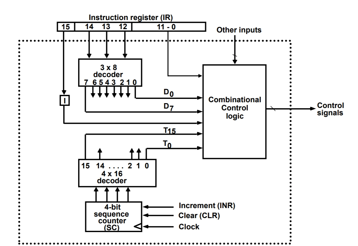
The output of the control logic circuit is as follows:
Signals to control the read and write inputs of memory
Signals to control the inputs of the eightregisters.
Signals to control the AC adder and logic circuit
Signals to control the S2, S1, and S0 to select a register for the bus
Signals to set, clear or complement the flip-flop
Control of Registers and Memory
Control inputs or signals of the registers are:
LD (load)
INR (increment)
CLR (clear)
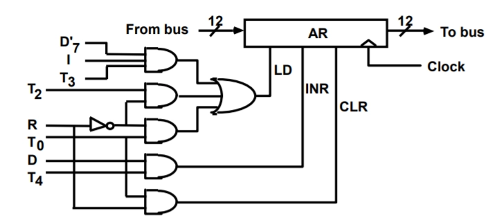
Let's consider the case of AR to understand the control of registers and memory.
If we want to derive the gate structure associated with the control input of AR, we consider all the statements that change the content of AR:
R'T0: AR ← PC
R`T2: AR ← IR (0-11)
D7`IT3 : AR ← M [AR]
RT0 : AR ← 0
D5T4: AR ← AR+1
1, 2, and 3 are responsible for transferring information from a register or memory to AR. The content of the source register memory is placed on the bus, and the content of the bus is transferred into AR by enabling its LD control input. 4 clears AR to 0 and 5 increments AR by one.
The control function can be combined into three boolean expressions as follows:
LD (AR) = R`T0 + R`T2 + D`7IT3 (load input of AR)
CLR (AR) = RT0 (clear of AR)
INR (AR) = D5T4 (increment input of AR)
The control gate logic associated with AR is shown below:
The read operation is recognized from the symbol ←M[AR]
Read = R`T1 + D`7IT3 + (D0 + D1 + D2 + D6)T4
The control logic gate for the above control function can be designed the same way we designed AR. In the above operation, addition refers to OR, and multiplication refers to AND. The output of the logic gates that implement the boolean expression above must be connected to the read input of memory.
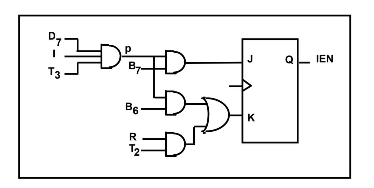
Control of single flip-flops
To understand the control of flip-flops, we will observe the control of IEN (Interrupt enable on) flip-flop. Now, the IEN may change as a result of the two instructions, ION and IOF
PB7: IEN ← 1
PB6: IEN ← 0
Where P = D7IT3
And B7 B6 are bits 7 and 6 of IR, respectively.
At the end of the interrupt cycle, IEN is cleared to 0
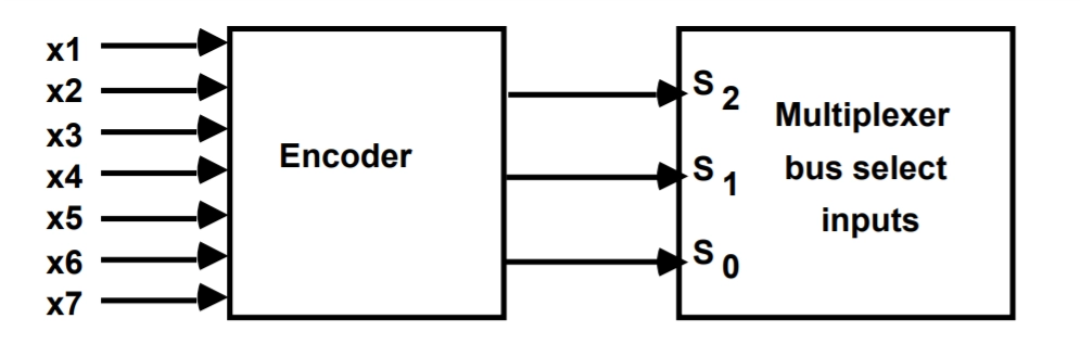
We can see in the above table that for each output value, there is a register selected. If we observe in the above table what events trigger S0 to be 1, we find that S0 is 1 when X1 or X3 or X5 or X7 is 1. Similarly, for S1 and S2. From this observation, we can deduce that each binary number is associated with a boolean variable (X1-X7), corresponding to the gate structure that must be active to select the register or memory for the bus.
The boolean function for the encoder can be written as
S0 = X1 + X3 + X5 + X7
S1 = X2 + X3 + X6 + X7
S2 = X4 + X5 + X6 + X7
It's necessary to find the control functions that place the corresponding register onto the bus to determine the logic for each encoder input. Let's find this for X1. First, we will scan all the register transfer statements and extract the statements having AR as a source. We get the following instructions after this:
D4T4 : PC ← AR
D5T5: PC ← AR
So the boolean expression for X1 becomes
X1 = D4T4 + D5T5
Similarly, we can find the gate logic for X2 to X7 for different registers.
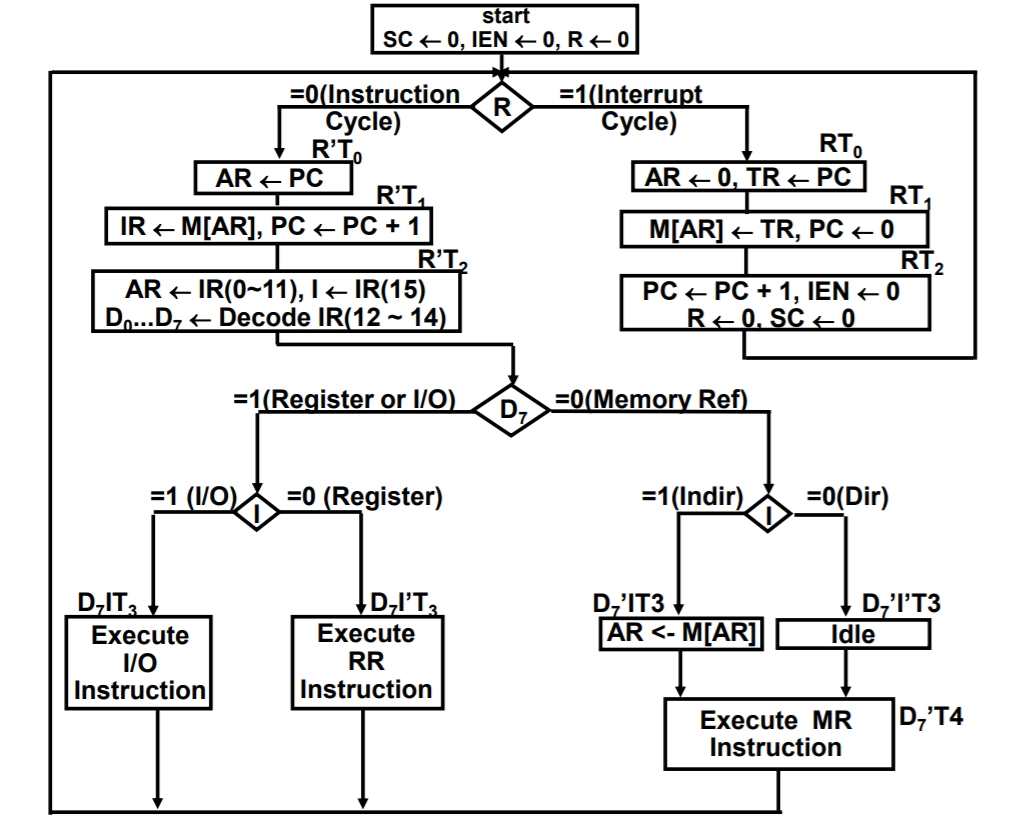
The instruction cycle is about how instruction is getting executed, and in the interrupt cycle, how Interrupt works when it occurs.
We start with Sequence counter set to 0, Interrupt enable set to 0, and R flip-flop set to 0.
R flip-flop is checked, which decides whether it is an instruction or an interrupt cycle.
When R is 0, then it is the instruction cycle.
At time R'T0, the PC contents are transferred to AR, which contains the address of the instruction to be executed.
At time R'T1, contents of memory pointed by AR are stored in IR. Along with that, PC is incremented by one as we have to shift to the next instruction. This step completes the fetch part of the process.
At time R'T2
decoding will take place from (12-14) bits of IR register which will generate the corresponding (D0-D7) bits
(0-11) bits of IR are copied to the AR register.
The 15th bit of the IR register is copied into I flip-flop.
After decoding, we check the D7 bit.
If the D7 bit is 1, it is either register or i/o instruction.
We check for I; if it is 1, then it is I/O instruction, and we immediately execute the I/O instruction at time T3. after this, we make the sequence counter 0.
If I value 0, then it is a register reference instruction, so we execute it at time T3 and set SC to 0
If the D7 bit is 0, (D0-D6) can be 1. So it becomes a memory reference instruction
We check for I bit; if it is 1, it is indirect addressing. So at time T3, the effective address is fetched from memory and stored in the AR register, and then after some time, memory reference instruction would get executed, and SC will be set to 0
If I bit 0, then it is direct addressing. So at time T3, we are supposed to do nothing, and then simply after that, memory reference instruction is executed, and SC is set to 0
After this, it goes back to the fetch part.
When R is 1, then it is an interrupt cycle.
At time RT0
store 0 in AR because interrupt cycle is similar to BSA (Branch and Save return Address), but the branching is fixed in case of Interrupt, and it is to be branched at address 0
address of next instruction which is stored in PC is stored in TR
At time RT1
Store the TR address in memory. We are storing the written address at address 0 here.
set the PC(Program Counter) to 0 because when Interrupt occurs then, we need to execute the service routine, which is at address 0
At time RT2, we
increment PC by 1
set IEN to 0 because earlier it was 0 due to interrupt cycle
set R to 0 because now it becomes our normal instruction cycle
SC is set to 0.
After this, it goes back to the normal instruction cycle execution.
Frequently Asked Questions
What are the steps for designing the computer?
System design is a step-wise process and has five phases in it. There are five steps for designing the computer. These steps are architectural Design, requirements Analysis, system Decomposition, testing, detailed design, and implementation. All these steps are compulsory and needed for computer design and architecture.
What is the structure of basic computer?
There are three essential components of the structure of the computer. The three components are a control processing unit (CPU), an input unit, and an output unit. in other words, the memory unit and control unit also form the basic structure of the computer.
What is computer architectural design?
Computer architecture refers to how a computer system's parts are organized and the meaning behind the actions that direct how it works. There are various forms of computer architecture, including Von-Neumann, Harvard, Instruction Set, Micro-, and System Design architectures. All these forms have their importance and functionality.
What is the importance of computer design?
Manual design drafting has been replaced by computer design, enabling design development, modification, and optimization. Experts can obtain more precise design representation with the aid of computers. It is employed at every engineering stage, product layout and conceptual design, and aids in imagining more intricate future construction projects.
Conclusion
In this article, we have extensively discussed the design of a basic computer, its hardware components and their use and the complete flowchart of the computer operation.
We hope that this blog has helped you enhance your knowledge regarding the design of a basic computer and if you would like to llearn more about Computer Organisation and Architecture, check out:


 9+ registered